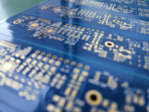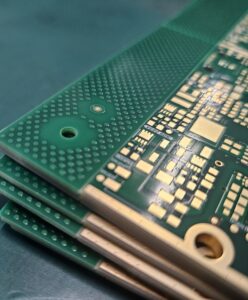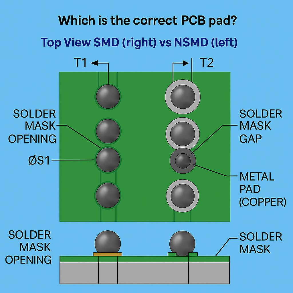
In PCB design, every detail matters — including the type of pads you use. Using BGA solder pads as an example, we compare two approaches: SMD (Solder Mask Defined) and NSMD (Non-Solder Mask Defined).
Choosing the right option can affect assembly accuracy, solder joint quality, and the overall reliability of the device.
What’s the difference?
SMD (Solder Mask Defined)
In this approach, the solder mask defines the size of the solderable area — the mask overlaps the copper edges, effectively “narrowing” the active pad surface.
✅ Advantages:
- higher mechanical robustness (the copper edge is partially protected),
- lower risk of solder spreading beyond the pad.
⚠️ Potential limitations:
- a smaller exposed area may reduce solder wetting,
- greater sensitivity to solder mask manufacturing tolerances (especially with fine pitch).
NSMD (Non-Solder Mask Defined)
Here, the entire copper pad surface is exposed, and the solder mask provides a clearance (gap) around the pad.
✅ Advantages:
- better wetting and solder “wrapping” around the pad edges,
- typically higher repeatability and placement accuracy for dense BGA layouts,
- more favorable stress distribution in the joint (often improving thermo-mechanical reliability).
⚠️ Potential limitations:
- greater exposure of copper edges (less “protection” than SMD),
- requires a properly selected solder mask clearance.
Practical takeaway
There is no single “always best” solution — pad selection should be based on:
- pitch and package type (especially BGA),
- PCB fabrication tolerances,
- reliability requirements and operating conditions,
- assembly and rework experience from similar builds.