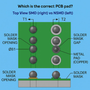
It is crucial to consider the manufacturer’s assembly recommendations already at the PCB design stage. These guidelines — available in component datasheets — often have a direct impact on the quality of the solder joints.
A good example is placing a BLGA package next to very small components such as 0201 or 0402. The recommended stencil thickness for these components can differ significantly: BLGA devices typically require a much thicker layer of solder paste compared to miniature passives. As a result, using a standard stencil optimized for “most components” may lead to unwanted voids under the BLGA solder joints.
If the PCB design is already completed and cannot be modified, one possible workaround is to use a stepped stencil with variable thickness. However, this approach also comes with technological limitations — for example, minimum spacing between components requiring different paste thicknesses. It is also worth noting that stepped stencils are several times more expensive than uniform-thickness stencils.
Therefore, a stepped stencil should be treated as a compromise solution. The best strategy is to prevent such issues early in the design phase — for instance, by placing sensitive components on opposite sides of the PCB or ensuring sufficient spacing between them.